Nanomaterials
Image

| Image

| Image

| Image

|
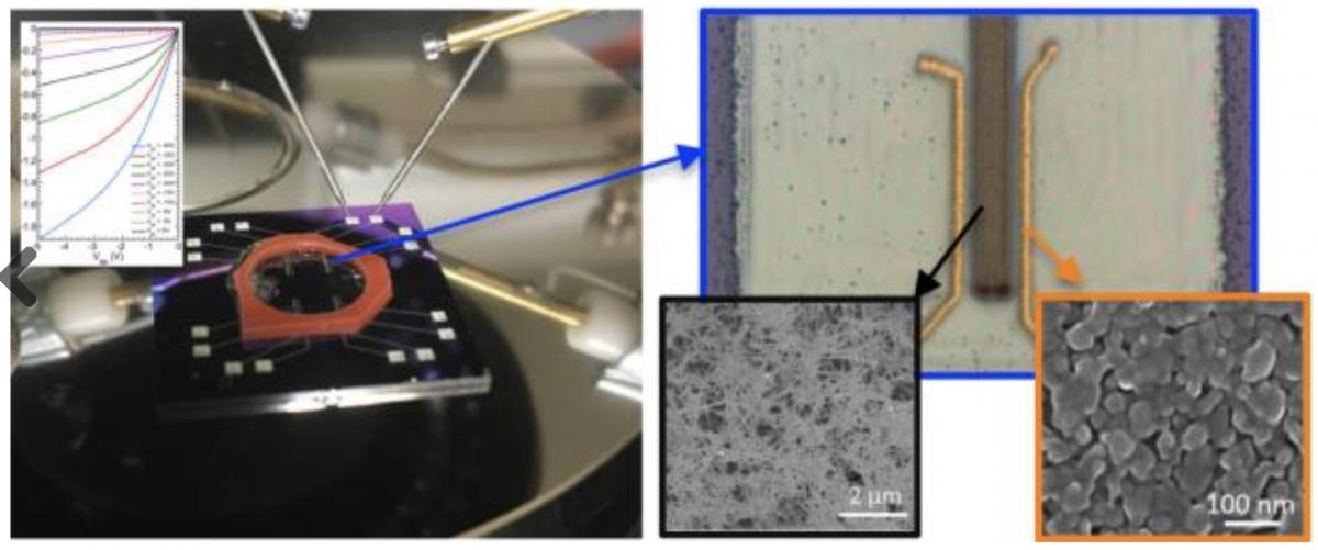
At the nanoscale, materials exhibit mechanical, electrical, and optical properties that are distinct from their macroscale assemblies. The Franklin group makes use of these unique properties to create electronics with new functions (e.g., extremely low voltage) and/or form factors (e.g., biocompatible, flexible). Rather than thinning down a bulk material to nanoscale dimensions, we focus on materials that are by their very nature 'nano.' These nanomaterials include carbon nanotubes (CNTs; 1 nm diameter cylindrical shell made from a single atomic sheet of carbon atoms bonded in a hexagonal (chicken wire) lattice), graphene (single atomic layer of carbon atoms in a hexagonal lattice), 2D transition metal dichalcogenides (TMDs; tri-layer stack of a transition metal sandwiched between two chalcogens, such as MoS2), and X-enes (single element in atomic sheet with a buckled hexagonal structure, such as phosphorene or silicene). Each of these one- or two-dimensional (1D or 2D) nanomaterials offers distinct advantages for certain applications with related scientific and engineering challenges. Our group works to harness these advantages while addressing the obstacles that keep them from enabling new functional technologies.

Low-Dimensional Nanoelectronics
Electrically, nanomaterials can provide near-ideal transport of electrons to yield devices that operate at lower power and push well-beyond the performance limits of current technologies. While there is much promise for pursing a new generation of devices from nanomaterials, there are key challenges that must be addressed in order to realize their full potential. Research in the Franklin group focuses on improving the crucial interfaces between nanomaterials and the needed contact, dielectric, and inert interfaces that a nanoelectronic device requires. High performance transistors, memory devices, and other passive devices are studied in the group. Examples and highlights from current research can be seen in our recent publications.
Printed Electronics
As the technological revolution marches on, the impact of electronics on our lives continues to increase. In the last decade, advances have been made in fabricating electronic components at extremely low cost for application-specific situations, especially with the continued growth of the Internet-of-Things (IoT). The most prominent device for enabling electronics is the transistor, which makes logical function and processing possible. Fabrication of high-performance transistors (that drive servers, smartphones, laptops, etc.) is done using extremely expensive vacuum and lithographric processing. While such processing has been fine-tuned and optimized for yielding aggressively scaled transistors that deliver superb performance, the cost precludes the fabrication of chips for bespoke (customer-specific) electronic applications.
Printing is one of the highest throughput and lowest cost fabrication approaches. Whether it is inkjet or roll-to-roll gravure, printing enables the deposition, removal, or curing of materials across a large surface in a single process step. Researchers have recently demonstrated the ability to fabricate transistors using printing processes for nearly every step. While such demonstrations are impressive and promising, the devices perform poorly and suffer from material stability issues. One of the research thrusts in the Franklin group is in the incorporation of nanomaterials to print transistors with improved performance and make them more compatible with a diversity of applications. We use an aerosol jet printing approach that makes it possibe to achieve printed line widths down to 10 µm and alignment of printed layers in the 1 µm range. Combining the versatility of aerosol jet printing with the benefits of nanomaterials is opening the way for a host of new and exciting applications and advancements.

Electronic Biosensors from Nanomaterials
As noted above, the printing of sensors provides a low-cost and highly customizable approach for enabling countless applications in this IoT era. This includes biosensors, such as immunoassays, used for the targeted detection of disease-specific antigens for rapid diagnosis. The intrinsic sensitivity of nanomaterials, when appropriately printed into such sensors, can provide tremendous advantages over the state-of-the-art. The Franklin group works collaboratively with researchers and clinicians from Duke's Biomedical Engineering (BME) department and School of Medicine to develop and study biosensors for point-of-care diagnostics, monitoring, and care.

With funding from the National Institutes of Health (NIH), biosensors are being pursued that have the potential to make a transformative impact on healthcare, including for the millions of people who do not have access to the costly and bulky medical equipment that many diagnostic procedures rely on. Exciting new discoveries and advancements in this area are happening each day in our lab and will be available in our publications very soon.

